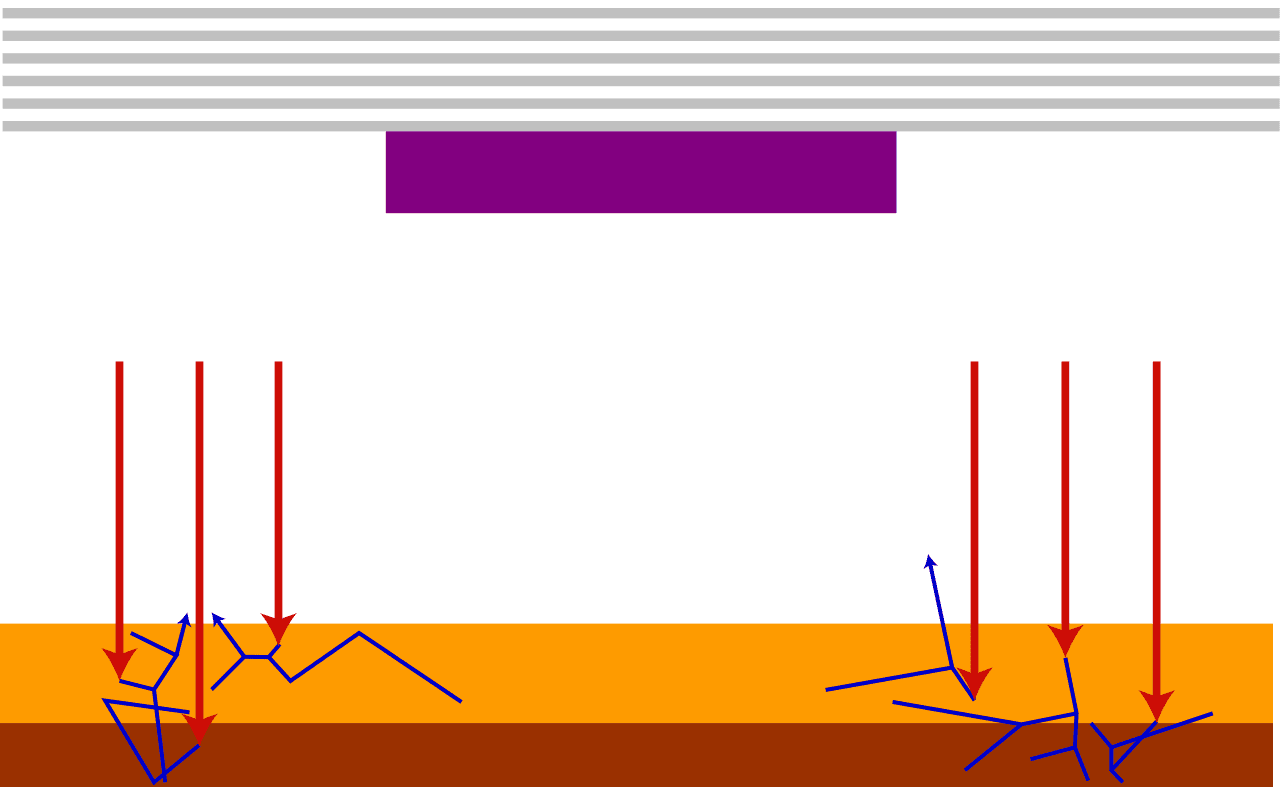
Extreme ultraviolet lithography (EUVL) is a groundbreaking technology in the semiconductor industry. It uses extreme ultraviolet light to create very fine patterns on silicon wafers, enabling the production of smaller and more powerful microchips. This advanced method supports Moore’s Law by printing intricate circuits with high resolution at nanometer scales.
EUV technology addresses the challenges of traditional photolithography, which struggles to keep up with the demands for smaller and faster chips. With a light wavelength of 13 nm, EUV allows for more precise and efficient manufacturing processes. Companies like ASML have developed advanced EUV lithography systems used by industry leaders to produce next-generation semiconductors.
EUV lithography has revolutionized the way we manufacture integrated circuits, making it a vital component in the continuous advancement of technology. Semiconductor manufacturers rely on this process to meet the increasing demands for better performance and efficiency in electronic devices. As the technology progresses, it promises even greater innovations in the world of microchips.
Image Credit: 2pem, CC BY-SA 3.0 https://creativecommons.org/licenses/by-sa/3.0, via Wikimedia Commons
This guide explains what EUV lithography is, how it works, and why it matters for the future of computing.
1. What Is EUV Lithography?
- Lithography is the process of using light to transfer patterns onto a silicon wafer (the “canvas” for microchips).
- EUV lithography uses extreme ultraviolet light at a 13.5 nm wavelength, which is much shorter than the deep ultraviolet (DUV) light (193 nm) used in older systems.
- A shorter wavelength means finer resolution, enabling manufacturers to print features as small as 5 nm and below (source: Nature Reviews Methods Primers).
2. How Does EUV Lithography Work?
The process involves several high-tech steps:
- EUV Light Source
- Generated by firing a high-powered laser at tiny droplets of tin.
- The collision creates plasma that emits EUV light at 13.5 nm.
- Optics and Mirrors
- Because EUV light is absorbed by air and glass, it must travel in a vacuum chamber.
- Special multilayer mirrors guide and focus the EUV light.
- Photomask
- A stencil-like plate containing the circuit design.
- The EUV light passes through the mask to project the pattern.
- Photoresist Layer
- A light-sensitive chemical coating on the silicon wafer.
- When exposed to EUV, parts of the resist change, allowing selective etching.
- Etching and Deposition
- The exposed wafer is processed to create the actual transistor and interconnect structures.
3. Why Is EUV Important?
- Enables Moore’s Law – Keeps chip scaling alive by allowing smaller transistors.
- Higher transistor density – More computing power in the same chip area.
- Energy efficiency – Smaller features reduce power consumption.
- Simplifies manufacturing – Replaces multiple patterning steps required in older DUV methods, cutting costs and complexity.
4. Current Challenges
Despite its promise, EUV lithography faces hurdles (source: Advanced Functional Materials):
- Photoresist limitations – Need materials that balance sensitivity, resolution, and line-edge roughness.
- Tool cost – Each EUV machine (from ASML, the sole supplier) costs over $150 million.
- Throughput – Generating enough EUV light for high-volume manufacturing remains challenging.
- Defect control – Even tiny imperfections can ruin chips at this scale.
5. Applications and Future Directions
- 5 nm and 3 nm chips – Already in production by companies like TSMC, Samsung, and Intel.
- High-NA EUV – Next-generation systems with higher numerical aperture optics promise 2 nm and beyond.
- Beyond semiconductors – EUV techniques are also being explored for metrology, materials science, and nanofabrication (source: Photonics.com).
6. The Bottom Line
Extreme Ultraviolet Lithography is one of the most advanced—and expensive—technologies in the world. It enables the semiconductor industry to keep pushing the boundaries of performance, efficiency, and miniaturization. While challenges remain, EUV is already shaping the chips that power today’s AI, smartphones, and data centers—and will continue to define the future of computing.
Advancing Chip Technology: EUV Lithography
Extreme Ultraviolet Lithography (EUV) is a cutting-edge technology revolutionizing semiconductor manufacturing. It’s a form of photolithography using extreme ultraviolet light with a wavelength of 13.5 nanometers, far shorter than deep ultraviolet (DUV) light used in traditional methods. This short wavelength allows for the creation of much smaller and more intricate patterns on silicon wafers, essential for producing the latest generation of advanced microchips.
EUV lithography is crucial for enabling Moore’s Law, the principle that the number of transistors on a microchip doubles approximately every two years. By allowing manufacturers to cram more transistors onto the same chip area, EUV lithography is fueling the development of smaller, faster, and more energy-efficient electronic devices like smartphones, computers, and data centers.
Why is EUV Lithography Important?
EUV lithography’s short wavelength light enables the creation of incredibly small features on microchips, pushing the boundaries of miniaturization. This leads to several key benefits:
- Smaller Transistors: EUV allows for the fabrication of transistors with dimensions as small as a few nanometers. Smaller transistors mean more can be packed onto a single chip, increasing performance and power efficiency.
- Improved Performance: The increased transistor density leads to faster and more powerful chips, capable of handling complex computations and data processing tasks.
- Enhanced Power Efficiency: Smaller transistors consume less power, resulting in longer battery life for mobile devices and reduced energy consumption for data centers.
Challenges and Solutions
EUV lithography, while groundbreaking, presents unique challenges:
- High Cost: EUV lithography machines are incredibly expensive, costing hundreds of millions of dollars each. This limits their adoption to leading-edge chip manufacturers with significant financial resources.
- Complex Technology: The technology involved in EUV lithography is highly complex, requiring sophisticated equipment, specialized masks, and precise control over the EUV light source.
- Low Throughput: EUV lithography has a lower throughput compared to traditional DUV lithography, meaning it takes longer to produce chips using this method.
Efforts are underway to address these challenges through technological advancements and process optimizations. Research focuses on improving the power output of EUV light sources, developing more efficient masks, and enhancing the overall throughput of EUV lithography systems.
Applications and Impact
EUV lithography is already used in the production of high-end microchips for various applications:
- Smartphones and Mobile Devices: EUV-enabled chips power the latest smartphones, tablets, and wearables, offering improved performance, longer battery life, and enhanced features.
- High-Performance Computing: EUV lithography is crucial for developing powerful processors and GPUs used in supercomputers, data centers, and artificial intelligence applications.
- Automotive Electronics: EUV-enabled chips are finding their way into advanced driver-assistance systems (ADAS), electric vehicles, and autonomous driving technologies.
- Medical Devices: EUV lithography contributes to the miniaturization and improvement of medical imaging equipment, implantable devices, and diagnostic tools.
Key Players in EUV Lithography
Currently, ASML Holding, a Dutch company, is the sole provider of EUV lithography systems for the semiconductor industry. Major chip manufacturers like TSMC, Samsung, and Intel rely on ASML’s EUV machines for their advanced chip production.
The Future of EUV Lithography
As research and development continue, the future of EUV lithography looks promising. Advancements in EUV technology are expected to lead to the production of even smaller and more powerful chips, pushing the boundaries of what’s possible in the world of electronics.
EUV Lithography in a Nutshell
| Feature | Description |
|---|---|
| Wavelength | 13.5 nanometers |
| Light source | Laser-produced plasma (LPP) |
| Benefits | Smaller transistors, improved performance, enhanced power efficiency |
| Challenges | High cost, complex technology, low throughput |
| Applications | Smartphones, high-performance computing, automotive electronics, medical devices |
| Key player | ASML Holding |
Key Takeaways
- EUVL uses extreme ultraviolet light to make detailed patterns on silicon wafers.
- It supports Moore’s Law by enabling the production of smaller and faster microchips.
- EUV lithography is essential for the future of semiconductor manufacturing.
Fundamentals of Extreme Ultraviolet Lithography
Semiconductors power everything from smartphones to supercomputers. As devices shrink and computing demands grow, the industry needs more precise ways to etch ever-smaller features onto silicon chips. Enter Extreme Ultraviolet (EUV) Lithography—a breakthrough technology that makes it possible to print patterns at the nanometer scale.
This section will explain the main principles, key components, and the process involved in extreme ultraviolet (EUV) lithography.
Principles of EUV Lithography
Extreme ultraviolet lithography uses very short wavelengths of 13.5 nanometers to etch patterns onto silicon wafers. These short wavelengths allow for much finer resolution, down to a few nanometers, which is ideal for creating advanced semiconductor components like transistors.
Because EUV light has high energy, it can achieve smaller feature sizes than traditional lithography methods. This makes EUV a strong candidate for manufacturing chips at the 7 nanometer node and below.
Components of EUV Systems
EUV systems contain several key components. First, the light source typically comes from a plasma, creating the necessary EUV light. This light must be collected and directed using multilayer mirrors, as regular mirrors can’t reflect this wavelength effectively.
Then, the light passes through a series of optical elements, such as reflective optics and projection optics, to focus it on the silicon wafer. Masks, including EUV masks, are used to transfer the desired patterns onto the wafer.
The EUV Process
The process of using EUV lithography involves several steps. First, a silicon wafer is coated with a photoresist material. The EUV light then exposes this material through the photomask. This exposure changes the chemical structure of the photoresist in the exposed areas.
Next, the exposed wafer undergoes development, where the photoresist is selectively removed. This creates a pattern on the wafer, which is subsequently etched to finalize the circuit design. The entire process requires precise machinery and conditions to maintain accuracy and resolution.
Using these detailed steps and components, EUV lithography allows for the production of smaller, faster, and more efficient semiconductor devices.
Frequently Asked Questions
This section covers the key aspects of extreme ultraviolet lithography (EUV) such as its capabilities in semiconductor manufacturing, leading companies, improvements over conventional systems, cost factors, differences from deep ultraviolet lithography, and future advancements.
What are the capabilities of extreme ultraviolet lithography in modern semiconductor manufacturing?
Extreme ultraviolet lithography (EUV) enables the creation of very small and intricate patterns on silicon wafers. This technology is crucial for producing advanced computer chips used in various devices. EUV lithography supports the development of smaller, faster, and more efficient chips that are essential in today’s digital products.
Which companies are leading in the development of extreme ultraviolet lithography technology?
ASML Holding is the primary company producing and selling EUV lithography systems. They are the leading supplier in this highly specialized market. Other notable companies involved in the research and development of EUV technology include Intel and TSMC.
How does high-NA extreme ultraviolet lithography improve upon conventional EUV systems?
High-NA (numerical aperture) EUV lithography enhances resolution and pattern accuracy. Compared to conventional EUV systems, high-NA systems achieve finer detail and greater precision in chip manufacturing. This improvement allows for the production of more advanced semiconductor devices with better performance and capabilities.
What are the cost factors associated with deploying extreme ultraviolet lithography machines?
The cost of deploying EUV lithography machines is high due to the complexity of the technology. Factors contributing to the costs include the advanced equipment needed, maintenance requirements, and the highly controlled cleanroom environments. These investments are necessary to ensure the precision and efficiency of semiconductor manufacturing processes.
What distinguishes deep ultraviolet (DUV) lithography from extreme ultraviolet (EUV) lithography?
DUV lithography uses light with longer wavelengths compared to EUV lithography. This results in less precise patterning capabilities than EUV, which employs shorter wavelengths for higher resolution. EUV can achieve finer patterns on silicon wafers, making it more suitable for producing smaller and more advanced chips.
What advancements are expected in extreme ultraviolet lithography for future technology nodes?
Future advancements in EUV lithography may focus on further improving resolution and throughput. Researchers are also exploring new materials and techniques to enhance the efficiency and capability of EUV systems. These developments aim to meet the increasing demands for smaller, faster, and more powerful semiconductor devices.

