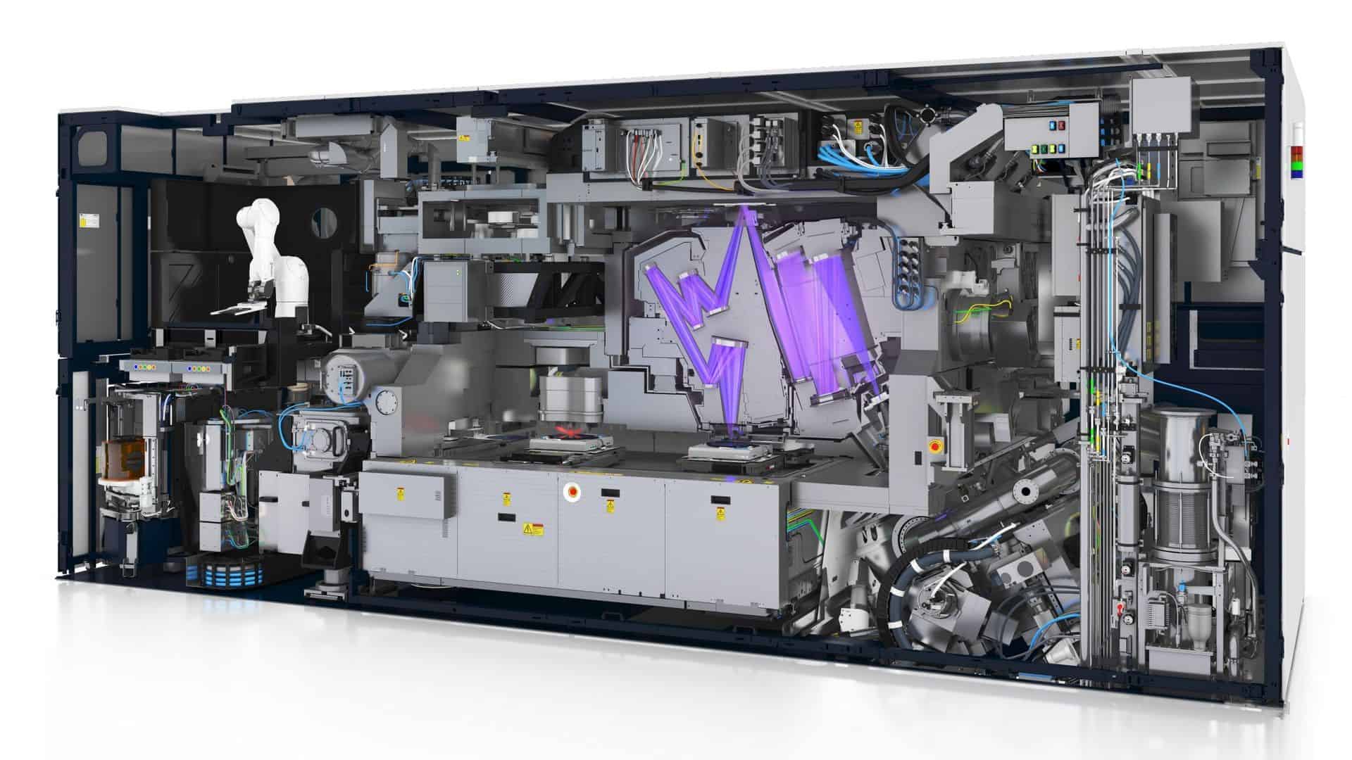
Extreme Ultraviolet (EUV) lithography machines, a cornerstone of modern semiconductor manufacturing, come with a substantial price tag. These complex machines are central to the production of cutting-edge chips, including those that are 5 nm in size and smaller. Understanding their cost is essential for grasping the financial dynamics of the semiconductor industry.
EUV Machine Cost Breakdown
| Component | Cost | Description |
|---|---|---|
| Lithography System: | $150 million – $400 million | This is the core of the EUV machine, responsible for projecting the light patterns onto the silicon wafer. The price varies depending on the specific model and its capabilities. |
| EUV Source: | $20 million – $50 million | This component generates the extreme ultraviolet light used in the lithography process. It is one of the most expensive parts of the machine. |
| Mask Aligner: | $10 million – $20 million | This component aligns the mask with the wafer to ensure precise patterning. |
| Stage & Wafer Handling: | $5 million – $10 million | This component moves the wafer into position under the EUV source and mask aligner. |
| Vacuum System: | $5 million – $10 million | This component maintains a vacuum environment inside the machine to prevent contamination. |
| Infrastructure: | $20 million – $50 million | This includes the cleanroom environment, power supply, and other infrastructure needed to operate the machine. |
| Installation & Maintenance: | $10 million – $20 million | This includes the cost of installing the machine and ongoing maintenance costs. |
| Total Cost: | $220 million – $500 million | This is the estimated total cost of an EUV machine, depending on the specific model and configuration. |
Additional Notes:
- The cost of EUV machines has been decreasing over time as technology advances and production becomes more efficient.
- However, EUV machines are still very expensive and represent a significant investment for chipmakers.
- The high cost of EUV machines is one of the factors that has led to the consolidation of the semiconductor industry, as only the largest chipmakers can afford to invest in the latest technology.
- The cost of EUV machines is expected to continue to decrease in the future, but they will likely remain expensive for the foreseeable future.
Sources:
- https://www.cnbc.com/2021/10/12/chip-machine-maker-asml-will-grow-into-a-500-billion-business.html
- https://www.reuters.com/technology/computer-chip-giant-asml-places-big-bets-tiny-future-2022-05-20/
- https://interestingengineering.com/innovation/new-award-winning-euv-lithography-enables-chips-5000-times-thinner-than-a-human-hair
The Financial Aspect of EUV Lithography Systems
Purchase Price
EUV machines represent a significant investment in the semiconductor manufacturing process. In 2022, the cost for an individual EUV machine was estimated to be nearly $200 million. This estimate aligns with specific figures released by ASML, a leading manufacturer of these systems. For instance, ASML disclosed that four of its EUV systems had a combined value of approximately €595 million (around $703 million), putting the cost of each machine at about €148.75 million ($175.75 million). Another perspective puts the price of each EUV tool at around $120 million. The variation in these estimates reflects differences in machine specifications and the rapid evolution of technology in this sector.
Operational Costs
In addition to their hefty purchase price, EUV machines are incredibly expensive to operate. Their complexity and the precision required in their functioning contribute to the high operational costs. This aspect underscores the significant financial commitment companies must make when incorporating EUV technology into their production lines.
Physical and Operational Characteristics
EUV machines are not only costly but also massive and intricate. Weighing about 200 tons and the size of a city bus, these machines are composed of over 100,000 parts and often require transportation in upwards of 40 freight containers. These characteristics add to the logistical and operational challenges, further contributing to the overall cost.
Understanding the Impact of EUV Machine Costs
The cost of EUV machines is a critical factor in the semiconductor industry, influencing production strategies and technological advancement. With their ability to create extremely small and precise elements on chips, these machines are indispensable for manufacturing the most advanced semiconductors. However, the financial barrier they represent also shapes the industry, determining which companies can compete at the highest levels of technology.
FAQs
- What is the cost of an EUV machine? EUV machines cost between $120 million to nearly $200 million, depending on the specifications and manufacturer.
- Why are EUV machines so expensive? The high cost is due to their complexity, the precision required in their operation, and the advanced technology they embody.
- What does an EUV machine do? EUV machines are used in semiconductor manufacturing to create extremely small and precise elements on chips, essential for advanced chip technology.
- How big are EUV machines? EUV machines are massive, weighing around 200 tons and comparable in size to a city bus.
- Are there any additional costs associated with EUV machines? Yes, besides the purchase price, EUV machines have high operational costs and require significant logistical planning for transportation and installation.
- How many parts does an EUV machine have? An EUV machine is made of more than 100,000 parts.
- Who manufactures EUV machines? ASML is one of the primary manufacturers of EUV lithography systems.
- How does the cost of EUV machines impact the semiconductor industry? The cost affects the industry by determining which companies can afford to invest in this advanced technology for chip production.
- Can the price of EUV machines vary? Yes, the price can vary based on the machine’s specifications and the rapid advancement of technology in this field.
- What is the significance of EUV technology in chip making? EUV technology is crucial for creating the most advanced and smallest elements on semiconductor chips, pushing the boundaries of chip performance and miniaturization.

