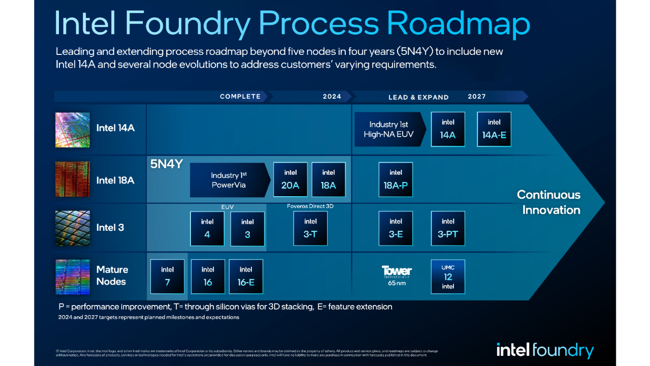
Intel is entering a pivotal era in its quest to reclaim leadership in semiconductor manufacturing. After stabilizing its roadmap with Intel 7 and Intel 4, the company is now pushing forward with 20A and 18A, the first nodes to feature its breakthrough RibbonFET transistor architecture and PowerVia backside power delivery. These advances mark not just incremental progress, but a fundamental shift in how chips are designed and powered.
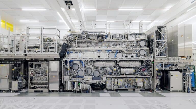
At the same time, Intel is the first to deploy High-NA EUV lithography from ASML, a next-generation tool that will enable denser, more efficient circuits than ever before. Together, these innovations reinforce Intel’s determination to extend Moore’s Law into the next decade, unlocking new levels of performance and energy efficiency that will power everything from AI to cloud infrastructure to next-generation PCs.
1. Where We Are Today: 18A (2025–2026)
Intel 18A is the company’s breakthrough node, representing:
- RibbonFET (gate-all-around transistors) – Intel’s first GAA transistor architecture.
- PowerVia (backside power delivery) – Separates power from signal routing, improving performance and efficiency.
- ASML High-NA EUV adoption – Intel is first to deploy High-NA EUV for tighter patterning.
This node is expected to power both Intel’s own CPUs and foundry customers’ designs starting in 2025–2026.
2. Beyond 18A: What Comes Next
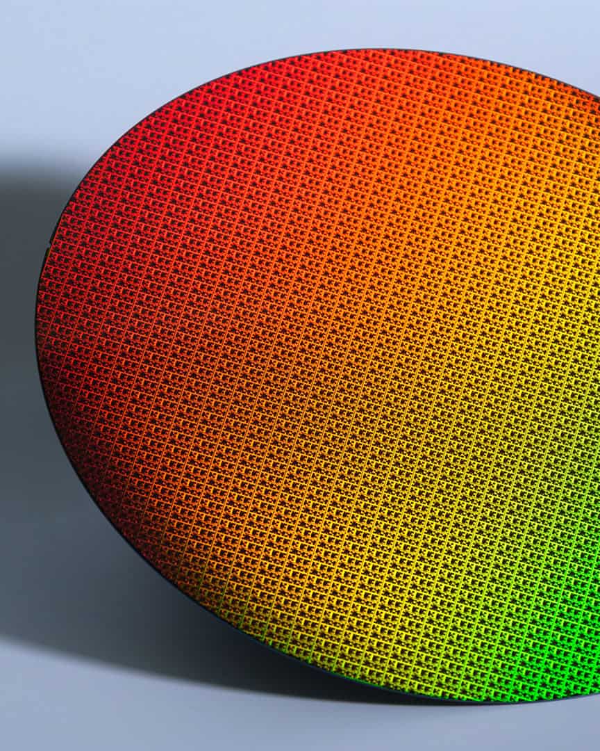
Intel hasn’t officially branded nodes beyond 18A, but based on industry trends and Intel’s disclosures, the roadmap likely includes:
14A (≈1.4nm class, ~2027)
- Refined RibbonFET with improved channel control.
- Optimized PowerVia with denser backside routing.
- Full-scale High-NA EUV adoption across multiple layers.
- Target: Compete with TSMC’s N14/N10-class nodes.
10A and Sub-10 Angstrom Era (2028–2030)
- Hybrid bonding at wafer scale for stacking logic-on-logic.
- 3D monolithic integration: true vertical stacking of transistors.
- New materials: Beyond silicon (e.g., 2D semiconductors like MoS₂, graphene, or germanium channels).
- Advanced interconnects: Optical or carbon nanotube-based wiring to reduce resistance.
3. Packaging as a Parallel Roadmap
Intel’s fab advances are tightly coupled with packaging:
- Foveros Direct – Direct copper-to-copper bonding for 3D stacking.
- EMIB evolution – Denser, lower-latency chiplet interconnects.
- System Technology Co-Optimization (STCO) – Designing chips as multi-die systems from the start.
Beyond 18A, packaging will become as critical as transistor scaling.
4. Challenges Intel Must Overcome
- Yield & cost: Sub-2nm nodes are extremely expensive; Intel must prove manufacturing maturity.
- Competition: TSMC and Samsung are racing toward similar timelines.
- Material & physics limits: Quantum tunneling, variability, and heat dissipation become major bottlenecks.
5. The Next Era: Post-Silicon Computing
Looking beyond 2030, Intel is researching:
- Quantum computing hardware (superconducting and spin qubits).
- Neuromorphic chips (brain-inspired architectures).
- Photonics integration for ultra-fast, low-power interconnects.
This suggests that “beyond 18A” is not just about shrinking transistors, but redefining computing architectures entirely.
✅ Summary:
Intel’s roadmap beyond 18A points toward 14A (~2027), 10A (~2028–2030), and eventually sub-angstrom nodes with new materials and 3D integration. At the same time, advanced packaging and post-silicon technologies will define the next era of semiconductor leadership.
Intel’s Ambitious Plans for the Future
Intel Process Roadmap Timeline
| Node | Estimated Launch | Key Innovations |
|---|---|---|
| Intel 7 | 2021–2022 | Refined FinFET, Alder Lake & Sapphire Rapids |
| Intel 4 | 2023 | First EUV node, Meteor Lake |
| Intel 3 | 2024–2025 | ~18% perf/watt gain over Intel 4, Granite Rapids |
| Intel 20A | 2024–2025 | RibbonFET (GAA), PowerVia (backside power) |
| Intel 18A | 2025–2026 | Refined RibbonFET + PowerVia, first High-NA EUV |
| Intel 14A | ~2027 | Enhanced GAA, expanded backside power delivery |
| Intel 10A | 2028–2029 | Full High-NA EUV adoption, 3D stacking, hybrid bonding |
| Sub-10A (Next-Gen) | 2030+ | New materials (2D semiconductors), optical interconnects, advanced 3D integration |
Intel is entering a new chapter under the leadership of CEO Lip-Bu Tan, who took the helm in 2025 after Pat Gelsinger’s tenure. With a sharpened strategy and renewed focus, Intel is doubling down on its process technology roadmap, extending well beyond the 18A node. This roadmap is central to Intel’s efforts to reclaim leadership in semiconductor manufacturing, and its success will shape the future of computing for consumers, enterprises, and the broader tech ecosystem.
What is 18A?
Intel 18A, expected to ramp in 2025–2026, represents a major inflection point. It introduces RibbonFET, Intel’s first Gate-All-Around (GAA) transistor, delivering better performance scaling and power efficiency compared to FinFET. It also debuts PowerVia, Intel’s backside power delivery network, which improves power distribution and reduces signal interference. Together, these innovations position 18A as the foundation for both Intel’s own CPUs and its foundry customers’ designs.
Beyond 18A: What We Know (and What We Don’t)
Intel has shared limited details about nodes after 18A, but several themes are clear:
- Refined RibbonFET: Continued optimization of GAA transistors for higher density and efficiency.
- Advanced PowerVia: Iterations of backside power delivery to further improve performance-per-watt.
- Specialized Nodes: Tailored processes optimized for AI, data center, mobile, and client workloads.
- High-NA EUV: Full-scale deployment of ASML’s next-generation lithography tools for tighter patterning.
Potential Timeline and Speculations
While Intel has not officially branded its post-18A nodes, industry watchers expect the following cadence:
| Process Node | Potential Timeframe | Notes |
|---|---|---|
| Intel 14A | ~2027 | Evolution of 18A with refined RibbonFET and PowerVia |
| Intel 10A | 2028–2029 | Likely to leverage High-NA EUV at scale, plus advanced 3D stacking |
| Sub-10A | 2030+ | Potential introduction of new materials (2D semiconductors, optical interconnects) |
What This Means for the Future
Intel’s aggressive roadmap signals a commitment to regaining semiconductor leadership. For consumers and businesses, this translates to:
- More Powerful Devices: Faster, more efficient PCs, servers, and AI accelerators.
- Cutting-Edge Features: Support for emerging standards and next-generation workloads.
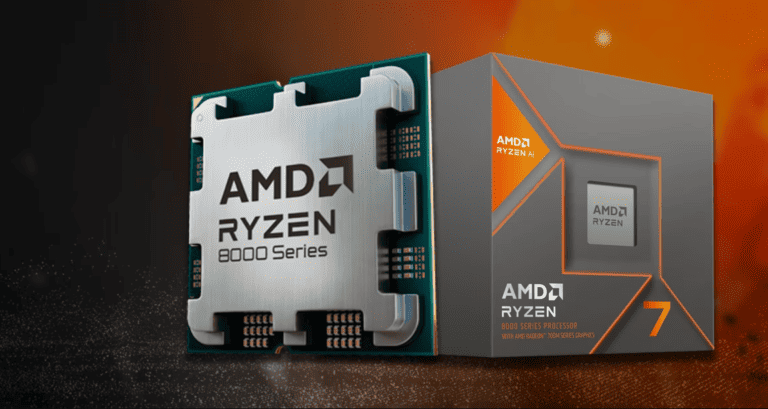
- Stronger Competition: A revitalized Intel will push rivals like TSMC, Samsung, and AMD to innovate faster.
While uncertainties remain, Intel’s roadmap beyond 18A looks promising. Its renewed focus on process technology and packaging innovation could spark a new wave of computing breakthroughs.
Key Takeaways
- Intel’s roadmap under CEO Lip-Bu Tan extends well beyond 18A, with 14A and 10A on the horizon.
- Next-generation lithography, RibbonFET, and PowerVia aim to sustain Moore’s Law into the 2030s.
- Advanced packaging (Foveros, EMIB, hybrid bonding) will be as important as transistor scaling.
Intel’s Strategic Vision for the Semiconductor Ecosystem
Intel’s strategy, first outlined under Pat Gelsinger as IDM 2.0 and now expanded by Lip-Bu Tan, positions the company as both a leading-edge chipmaker and a global foundry partner. Intel Foundry Services (IFS) remains central to this vision, offering advanced manufacturing to external customers while strengthening the resilience of the semiconductor supply chain.
With 20A and 18A as near-term milestones, Intel is also investing heavily in packaging, ecosystem partnerships, and advanced design enablement. By opening its fabs to more customers and collaborating across the industry, Intel is positioning itself as a cornerstone of the global semiconductor ecosystem.
Innovations and Advancements in Intel’s Roadmap
Intel’s roadmap beyond 18A suggests a future defined by new transistor architectures, advanced packaging, and system-level co-optimization. These innovations are designed not only to improve raw performance, but also to meet the efficiency demands of AI, cloud, and edge computing.
Next-Generation Process Nodes and Their Impact
Intel 3, 20A, and 18A set the stage for the next leap forward, with Intel 14A and 10A expected to follow later in the decade. Each node brings tighter transistor density, better performance-per-watt, and greater scalability for AI and HPC workloads. By 2030, Intel aims to transition into sub-10 angstrom technologies, where new materials and 3D integration will be essential.
Intel’s Product Pipeline and Technological Breakthroughs
On the product side, Intel continues to roll out new client and data center CPUs. Arrow Lake and Lunar Lake are set to bring efficiency and AI acceleration to PCs, while Granite Rapids and Sierra Forest target next-gen data centers with scalable performance. Advanced packaging technologies like Foveros Direct and EMIB are enabling chiplet-based designs that integrate compute, memory, and accelerators more tightly than ever before.
Together, these breakthroughs highlight Intel’s determination to remain at the forefront of both process technology and product innovation, ensuring competitiveness across markets from PCs to hyperscale data centers.
Frequently Asked Questions
Intel’s roadmap promises significant advancements in computing by 2030. With detailed milestones through 18A and plans for 14A and beyond, Intel’s innovations will continue to shape the future of technology. Here are answers to some common questions:
What technological advancements can we expect in Intel’s roadmap by 2030?
By 2030, Intel is expected to move beyond 18A into 14A, 10A, and potentially sub-10 angstrom nodes. These will feature refined GAA transistors, advanced backside power delivery, and possibly new materials like 2D semiconductors. The result: higher performance, lower power, and greater scalability for AI and HPC.
How will Intel’s advanced packaging technology evolve?
Intel is pushing forward with Foveros Direct and EMIB, which enable high-density, low-latency interconnects between chiplets. Future packaging will likely incorporate hybrid bonding and wafer-on-wafer stacking, unlocking new levels of system performance.
What are the major milestones in Intel’s product roadmap up to 2026?
Key milestones include Intel 3 for data centers, 20A and 18A for CPUs and foundry customers, and the launches of Arrow Lake, Lunar Lake, Granite Rapids, and Sierra Forest. These products will showcase Intel’s advanced nodes and packaging innovations.
What can users anticipate from the upcoming Intel Arrow Lake processors?
Arrow Lake processors are expected to deliver major gains in efficiency, graphics, and AI acceleration, leveraging Intel’s latest process technology and packaging. They are positioned as the next big step for client PCs, arriving in the mid-2020s.
How does Intel’s 20A technology compare to its predecessors?
Intel 20A introduces RibbonFET and PowerVia for the first time, marking a transition from FinFET to GAA transistors. Compared to Intel 4 and Intel 3, 20A offers dramatically improved power efficiency and transistor density, setting the stage for 18A and beyond.
What innovations is Intel planning to implement in the near future?
Near-term innovations include High-NA EUV lithography, advanced packaging (Foveros/EMIB), and specialized process nodes for AI and data centers. These technologies will allow Intel to sustain Moore’s Law while enabling new computing paradigms.

