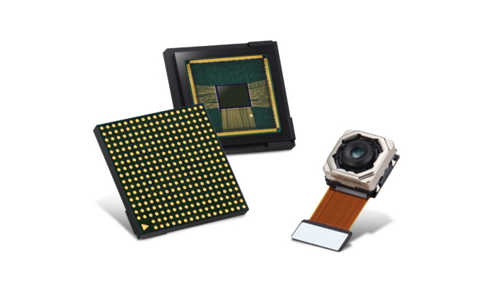
Samsung is making big advancements in the semiconductor industry, especially with its new image sensor chips. These chips capture light better, which is important for low-light settings where there isn’t much light. The introduction of chips with 0.7μm pixels breaks old limits and shows Samsung’s commitment to pushing technological boundaries. Samsung is not only improving image sensors but also focusing on environmental sustainability.
Recently, some of its memory products and automotive LED packages earned global recognition for reducing carbon emissions. Samsung’s System LSI products also received carbon footprint certification from the Carbon Trust, showing the company’s efforts to create eco-friendly technology. Samsung’s ability to innovate in technology and environmental sustainability shows its leadership in the global semiconductor market. The company is always looking for new ways to capture light and reduce emissions, making significant contributions to the industry and the planet.
Samsung’s Innovations in Imaging Technology
Samsung has consistently established itself as a leader in the smartphone industry, particularly through groundbreaking innovations in camera technology. From revolutionary image sensors to cutting-edge AI integration, Samsung continues to push the boundaries of what smartphone cameras can achieve.
Current Camera Technologies
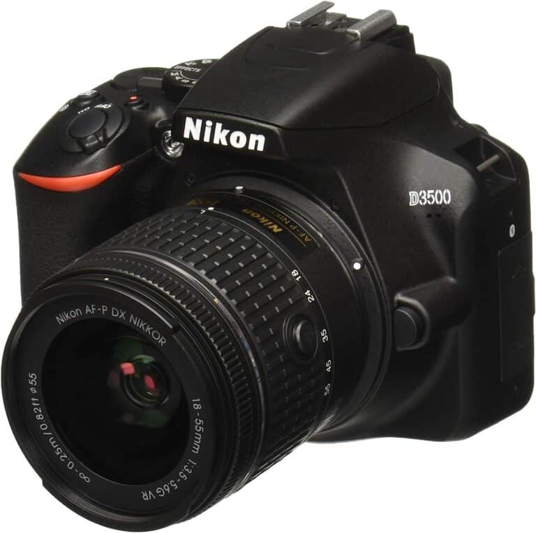
Multi-Camera Systems and Computational Photography
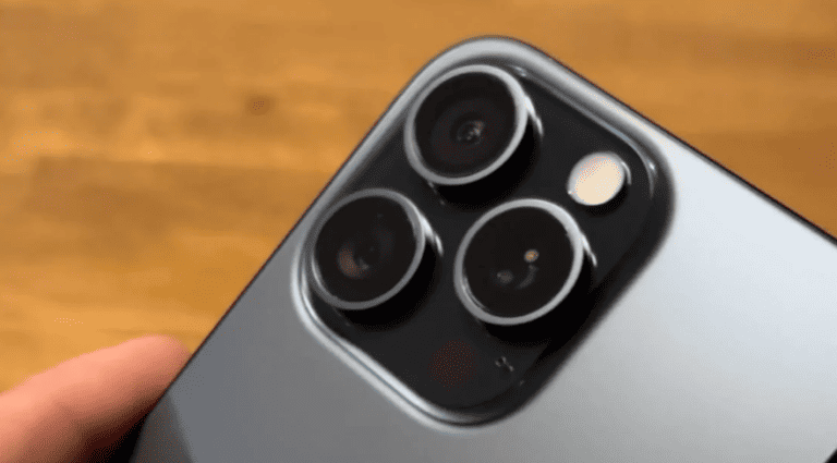
Samsung is at the forefront of multi-camera technology research. As noted by industry experts, “The most talked about topic in computational photography is multi-camera technology. Researchers and companies are still researching what camera setup is best” (source: ZDNet).
Galaxy S25 Series Innovations
The latest Galaxy S25 series showcases Samsung’s commitment to camera excellence with:
- 50MP Ultra-Wide Camera Sensor: Provides exceptional detail and clarity across wide-angle shots
- AI Remosaic Technology: Allows users to capture high-resolution photos from any distance
- AI-Based Multi-Frame Processing (MFP): Automatically optimizes image quality based on shooting environment and distance while precisely distinguishing between moving and static subjects
(source: Samsung Mobile Press)
Revolutionary AI Integration
Humanoid Sensors – The Future of Camera Technology
Samsung is developing groundbreaking “Humanoid Sensors” technology, which aims to integrate artificial intelligence directly into dedicated camera sensor chips. This innovative approach is designed to replicate human vision capabilities and represents a significant leap forward in imaging technology.
Key Features of Humanoid Sensors:
- Direct AI integration into camera image sensors
- Enhanced image quality through intelligent processing
- Faster real-time image processing capabilities
- Advanced object and scene recognition features
- Human-like visual perception and analysis
Expected Timeline: Samsung plans to roll out devices featuring this technology by 2027 (source: Korea Tech Today).
Current AI Camera Innovations
Samsung’s current AI camera implementations focus on:
- Intelligent Scene Recognition: Automatically detecting and optimizing for different shooting scenarios
- Real-time Image Enhancement: AI algorithms that improve image quality during capture
- Smart Object Tracking: Advanced focusing systems that follow subjects intelligently
- Adaptive Processing: Dynamic adjustment of camera settings based on environmental conditions
Research and Development Focus
Mobile Processor Innovation for Imaging
Samsung Research America emphasizes that “Smartphone camera quality continues to be deeply important to consumers” and recognizes that “customer demand for continued quality improvements and new features is driving the need for breakthroughs in computational imaging and AI camera” (source: Samsung Research America).
Computational Imaging Breakthroughs
Samsung’s research focuses on several key areas:
- Advanced Image Sensors: Developing larger, more sensitive sensors with improved low-light performance
- AI-Powered Processing: Creating more sophisticated algorithms for real-time image enhancement
- Multi-Spectral Imaging: Exploring beyond visible light for enhanced imaging capabilities
- Edge Computing: Bringing more processing power directly to the camera hardware
Impact on the Industry
Samsung’s imaging innovations are setting new standards for:
- Image Quality: Consistently delivering professional-grade photos from mobile devices
- User Experience: Simplifying photography through intelligent automation
- Technology Integration: Seamlessly combining hardware and software innovations
- Future Vision: Leading the industry toward AI-integrated imaging solutions
Looking Ahead: 2027 and Beyond
Samsung’s vision for the future of imaging technology centers around the Humanoid Sensors initiative, which promises to “revolutionize camera sensors with integrated AI chips, aiming to replicate human vision” (source: Fizzzoom).
This technology represents a fundamental shift from traditional image processing to intelligent, human-like visual perception directly embedded in camera hardware.
Conclusion
Samsung’s continuous innovation in imaging technology demonstrates the company’s commitment to pushing the boundaries of what’s possible in mobile photography. From current AI-enhanced multi-camera systems to the revolutionary Humanoid Sensors planned for 2027, Samsung is shaping the future of how we capture and process images.
The integration of artificial intelligence directly into camera sensors represents not just an incremental improvement, but a paradigm shift that could redefine mobile photography and set new standards for the entire industry.
Pushing Boundaries in Digital Imaging
Isocell Sensors
Samsung’s Isocell technology is a game-changer in mobile photography. It enhances light sensitivity and color fidelity in smartphone cameras, resulting in brighter, more vibrant images even in low-light conditions.
Nonacell Technology
Nonacell takes pixel-binning to the next level. By merging nine pixels into one, it significantly improves low-light performance, producing stunning night shots with reduced noise.
Adaptive Pixel Technology
This innovative technology combines the best of high-resolution and low-light photography. It uses two sets of pixels: one for detailed daytime shots and another for capturing more light in low-light scenarios.
Space Zoom and Zoom Lock
Samsung’s Space Zoom technology combines optical and digital zoom to achieve incredible magnification without sacrificing image quality. Zoom Lock helps stabilize the image at high zoom levels, ensuring sharper shots.
Director’s View
This feature allows users to record videos from multiple camera angles simultaneously. It offers a professional-level video experience, giving you more control and creative options.
AI-Powered Image Processing
Samsung employs sophisticated AI algorithms to enhance image quality. These algorithms optimize color, sharpness, and noise reduction, resulting in more lifelike and detailed photos.
Comparison of Samsung’s Imaging Technologies
| Technology | Description | Benefits |
|---|---|---|
| Isocell | Pixel isolation technology | Improved light sensitivity, color fidelity |
| Nonacell | 9-in-1 pixel binning | Enhanced low-light performance |
| Adaptive Pixel | Dual-pixel architecture | High-resolution and low-light optimization |
| Space Zoom | Hybrid zoom technology | High magnification with image quality |
| Zoom Lock | Zoom stabilization | Sharper photos at high zoom levels |
| Director’s View | Multi-camera recording | Professional-level video experience |
| AI-Powered Image Processing | AI-based image enhancement | Optimized color, sharpness, noise reduction |
Key Takeaways
- Samsung leads in image sensor technology with chips capturing light effectively.
- Environmentally-friendly efforts have led to recognition for reduced carbon emissions.
- Global certifications validate Samsung’s sustainable semiconductor advancements.
Samsung’s Semiconductor Advancements
Samsung has made significant strides in semiconductor technology, enabling innovations in various fields like photography, AI, and IoT. These advancements have widespread implications, from high-performance computing to enhanced consumer electronics.
Leading Edge Chip Innovation
Samsung Electronics leads in chip innovation through constant investment and research. Their manufacturing facilities, especially in Texas, play a crucial role. Samsung has invested billions in their fabs in Austin and Taylor, pushing forward semiconductor production capabilities.
Using technologies like Tetrapixel and Nanopixel, Samsung achieves higher resolution and better image quality in devices. These innovations help mobile cameras capture more details and manage light effectively.
Their collaboration with entities like Intel showcases their drive to dominate the semiconductor landscape.
Illumination Technology and LED Development
Samsung’s LED component solutions are impacting various sectors. Their products like LH231B, LM101B, and LH181B offer high efficacy and reliability. Samsung’s LEDs are used in items ranging from 1W-Class to 5W-Class, providing excellent light output.
Their CSP Technology enhances mid-power LEDs, making them suitable for diverse applications.
Samsung’s LED solutions cater to automobile lighting, consumer electronics, and IoT devices, highlighting their market impact. Luminaire designers find these components useful for designing energy-efficient lights.
Market Impact and Applications
Samsung’s advancements have substantial market effects. Their investments in semiconductor manufacturing facilities in Texas have boosted local economies and job creation. The company receives significant funding under the CHIPS and Science Act, emphasizing its importance in the industry.
Samsung chips are vital in numerous applications across sectors. From automotive technology to digital consumer products, these chips enhance performance and reliability. They also contribute to IoT developments, supporting a connected world.
The high-performance chips are crucial for AI, high-speed computing, and 5G communications, showcasing Samsung’s indispensable role in modern technology.
Frequently Asked Questions
Samsung’s advanced chips are making significant strides in improving low-light photography and enhancing camera functionalities. The collaboration between Samsung and U.S. initiatives is also crucial in the production of high-quality semiconductor chips.
How is Samsung’s AI technology enhancing photography capabilities in low light conditions?
Samsung’s AI technology adjusts settings automatically to capture better images in low-light conditions. This is achieved by optimizing exposure and reducing noise, allowing for clearer and more detailed photos. Newer image sensors with smaller pixels also boost performance in these settings.
What improvements have been made in the Samsung S23 Ultra AI camera’s zoom function?
The Samsung S23 Ultra features enhanced AI-driven zoom capabilities. The AI helps stabilize the image and refines details at higher zoom levels. This results in sharper, clearer images even when zooming in significantly on distant objects.
In what ways does the Pro mode on Samsung Android devices affect lunar photography settings?
The Pro mode in Samsung Android devices allows manual adjustments for better lunar photography. Users can control settings like ISO, shutter speed, and focus to capture detailed and vivid images of the moon. These adjustments help in achieving professional-quality images from a smartphone.
Has Samsung provided an official statement regarding the authenticity of the moon images captured by its devices?
Yes, Samsung has addressed concerns about the authenticity of moon images captured by its devices. The company has assured that the images are a result of advanced AI image processing and not fake enhancements. This ensures users get a realistic and high-quality representation of the moon.
What role does the Texas Chips Act play in the production of Samsung’s semiconductor chips?
The Texas Chips Act supports the expansion and innovation of semiconductor manufacturing in Texas. Samsung benefits from this act by receiving funding and resources to build and operate semiconductor plants. This helps Samsung maintain its leadership in semiconductor technology.
Which company is responsible for manufacturing the chips used in Samsung’s devices?
Samsung itself manufactures the chips used in its devices. The company has state-of-the-art facilities in Texas and other locations that produce advanced semiconductor chips. This vertical integration helps Samsung control the quality and innovation of its products.

