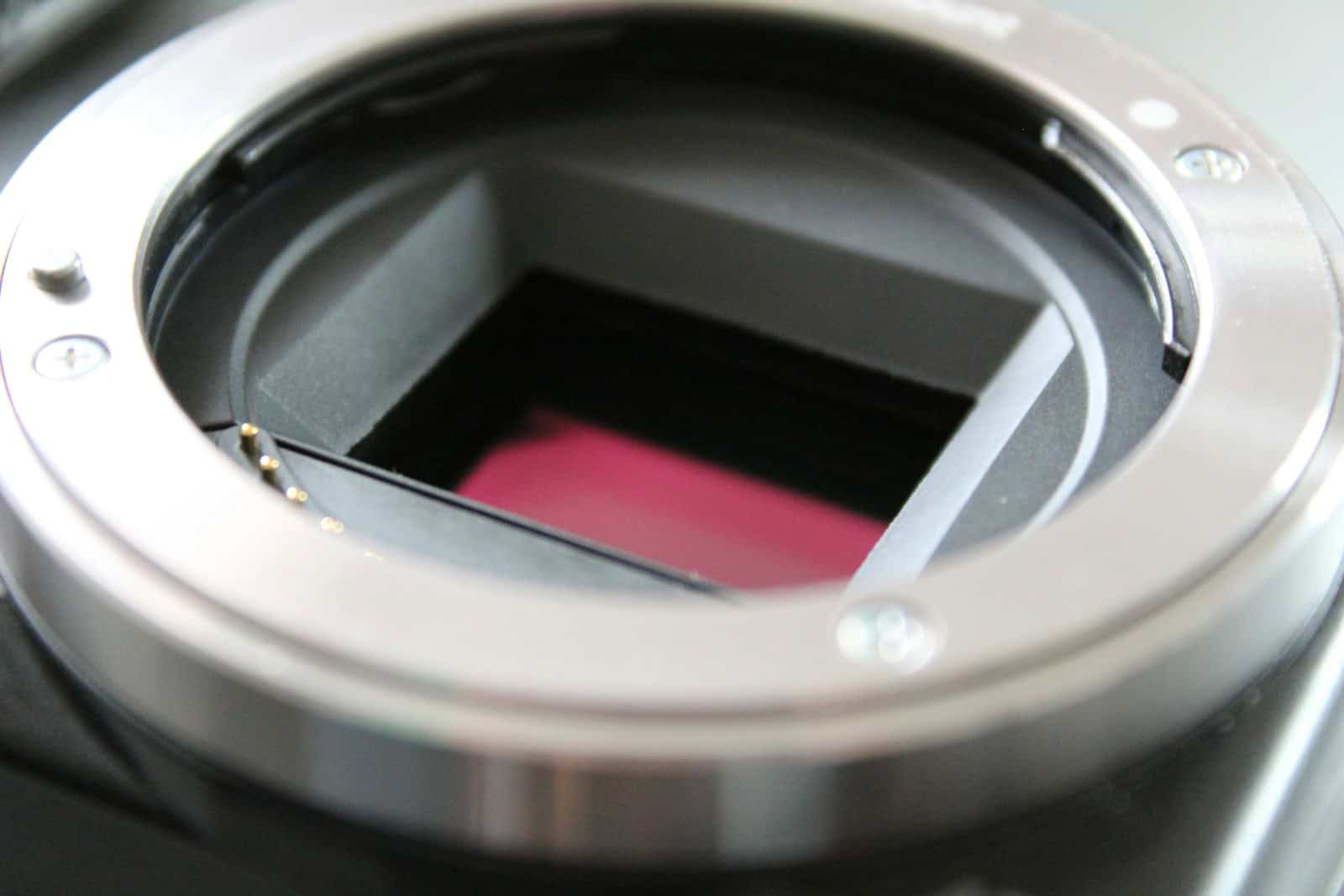
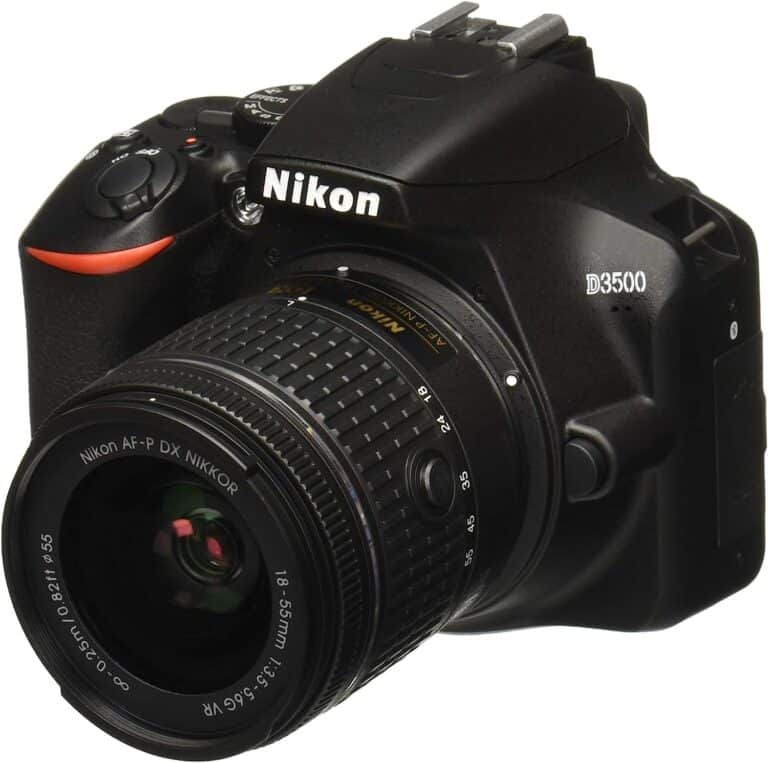
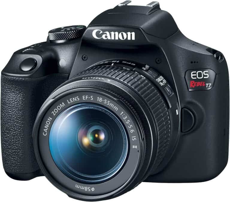
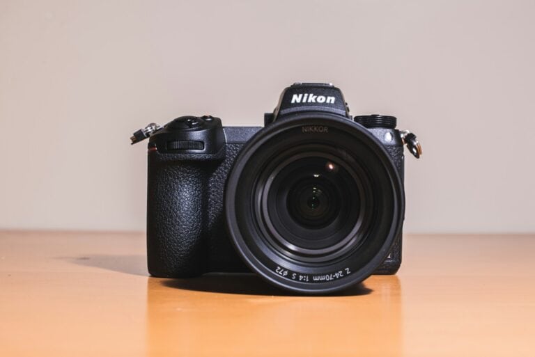
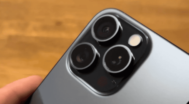
Digital cameras capture images using tiny sensors that turn light into electronic signals. A CMOS image sensor is a semiconductor device that converts incoming light into digital images using thousands of photon detectors on a chip surface. These sensors measure both the color and brightness of light to create the photos people see on their camera screens.
CMOS stands for Complementary Metal-Oxide-Semiconductor. This technology appears in nearly every modern digital camera, from smartphones to professional equipment. Each sensor contains millions of tiny pixels that work together to record what the camera sees.
Understanding how these sensors work helps photographers make better choices about their equipment. The technology affects image quality, battery life, and camera performance in ways that matter for both casual users and serious photographers.
CMOS Image Sensors
CMOS (Complementary Metal-Oxide-Semiconductor) image sensors have revolutionized modern digital imaging, powering everything from smartphone cameras to advanced scientific instruments. This comprehensive guide explores their fundamentals, technology, and performance characteristics.
Introduction to CMOS Image Sensors
CMOS image sensors are fabricated in “standard” CMOS technologies. Their widespread adoption stems from several key advantages over traditional CCD (Charge-Coupled Device) sensors, including the ability to integrate analog and digital circuits with the sensor, resulting in fewer chips used in imaging systems, lower power dissipation, faster readout speeds, and more programmability.
Fundamental Operating Principles
Photon to Signal Conversion
Digital image sensors work by converting photons into electrical signals, and thus images. The basic process involves:
- Photon Absorption: Light photons strike the sensor’s photodiodes
- Charge Generation: Photons create electron-hole pairs in the silicon substrate
- Charge Collection: Generated electrons accumulate in potential wells
- Signal Readout: Accumulated charge is converted to voltage and read out
Pixel Architecture
Each pixel in a CMOS sensor typically contains:
- Photodiode: Converts light to electrical charge
- Transfer Gate: Controls charge transfer from photodiode
- Floating Diffusion: Converts charge to voltage
- Reset Transistor: Clears accumulated charge
- Source Follower: Amplifies the signal
- Row Select Transistor: Enables pixel readout
CMOS vs. CCD Technology
Key Differences
CCD Sensors:
- Sequential charge transfer through shift registers
- High-quality, uniform readout
- Higher power consumption
- More complex manufacturing process
CMOS Sensors:
- Individual pixel amplification and readout
- Random access capability
- Lower power consumption
- Easier integration with processing circuits
Performance Trade-offs
CMOS Advantages:
- Lower power consumption
- Faster readout speeds
- System-on-chip integration
- Cost-effective manufacturing
- Better suited for portable devices
CCD Advantages:
- Superior image quality (historically)
- Better low-light performance
- Less noise in certain conditions
- More uniform pixel response
Advanced CMOS Technologies
Modern Enhancements
Contemporary CMOS sensors incorporate new functionalities including high dynamic range, biometric capabilities, and other specialized features. Key technological advances include:
Backside Illumination (BSI):
- Improved light collection efficiency
- Better low-light performance
- Reduced crosstalk between pixels
Stacked Sensor Design:
- Separate processing and imaging layers
- Enhanced functionality integration
- Improved performance density
Advanced Pixel Architectures:
- Dual conversion gain pixels
- Shared pixel designs
- In-pixel analog-to-digital conversion
Performance Characteristics
Key Performance Metrics
Sensitivity:
- Quantum efficiency across different wavelengths
- Signal-to-noise ratio
- Minimum detectable light levels
Dynamic Range:
- Maximum contrast ratio between brightest and darkest areas
- Linear and logarithmic response modes
- Multi-exposure techniques
Speed:
- Frame rate capabilities
- Readout speed
- Processing latency
Image Quality:
- Noise characteristics
- Color accuracy
- Spatial resolution
- Temporal noise
Factors Affecting Performance
Pixel Size:
- Larger pixels: Better light sensitivity, lower noise
- Smaller pixels: Higher resolution, more compact sensors
Fill Factor:
- Percentage of pixel area sensitive to light
- Affects overall sensitivity and image quality
Manufacturing Process:
- Node size impacts pixel design flexibility
- Process variations affect uniformity
Applications and Use Cases
CMOS image sensors are a critical component in modern imaging technology, offering a blend of high performance, low power consumption, and cost-effectiveness. Their ability to integrate additional processing functions on the same chip has revolutionized the design and functionality of digital cameras, smartphones, automotive systems, medical devices, and more.
Primary Applications
Consumer Electronics:
- Smartphone and tablet cameras
- Digital cameras and camcorders
- Laptop and desktop webcams
- Gaming and VR systems
Automotive:
- Backup and surround-view cameras
- Advanced driver assistance systems (ADAS)
- Autonomous vehicle perception
- Interior monitoring systems
Medical and Scientific:
- Endoscopy and surgical imaging
- Microscopy systems
- X-ray and radiographic imaging
- Fluorescence imaging
Industrial and Security:
- Machine vision systems
- Quality control and inspection
- Security and surveillance cameras
- Barcode and QR code readers
Emerging Applications:
- Augmented reality devices
- Drone and aerial photography
- Internet of Things (IoT) devices
- Biometric authentication systems
Design Considerations and Optimization
System Integration
On-Chip Processing:
- Image signal processing (ISP)
- Analog-to-digital conversion
- Timing and control circuits
- Interface protocols
Power Management:
- Sleep and standby modes
- Dynamic power scaling
- Optimized readout schemes
- Voltage regulation
Specialized Designs
Scientific Applications:
- Low noise optimization
- Extended dynamic range
- Specialized spectral responses
- Radiation hardening
Automotive Requirements:
- Wide temperature operation
- Functional safety compliance
- Automotive-grade reliability
- EMI/EMC considerations
Future Trends and Developments
Emerging Technologies
Computational Photography:
- AI-enhanced image processing
- Multi-frame noise reduction
- Super-resolution techniques
- Depth sensing integration
Advanced Materials:
- Organic photodiodes
- Perovskite sensors
- Quantum dot integration
- Novel semiconductor materials
3D Integration:
- Multi-layer sensor stacking
- Through-silicon vias (TSV)
- Heterogeneous integration
- System-in-package (SiP) designs
Conclusion
CMOS image sensors have fundamentally transformed digital imaging through their unique combination of performance, power efficiency, and integration capabilities. As technology continues to advance, these sensors are becoming increasingly sophisticated, enabling new applications and improving existing ones across diverse industries. Understanding their fundamental principles, technological advantages, and performance characteristics is essential for anyone working with modern imaging systems.
The continued evolution of CMOS technology, driven by advances in semiconductor manufacturing and system integration, promises even more exciting developments in the future of digital imaging.
Key Takeaways
- CMOS image sensors convert light into digital images using millions of tiny photon detectors on a semiconductor chip
- These sensors are found in nearly all modern digital cameras and smartphones
- Learning about CMOS technology helps users understand their camera’s performance and capabilities
Frequently Asked Questions
CMOS image sensors convert light into electrical signals through photodetection and charge amplification. They offer faster processing and lower power consumption compared to CCD sensors, with costs influenced by resolution, manufacturing complexity, and market demand.
How do CMOS image sensors function?
CMOS image sensors work by converting light into electrical signals through the photoelectric effect. Each pixel contains a photodetector that accumulates electrical charge when photons strike it.
The amount of charge collected corresponds directly to the light intensity hitting that pixel. Individual transistors within each pixel amplify this charge and convert it to a voltage signal.
The sensor includes analog-to-digital converters that transform these voltage signals into digital data. This digital information represents the brightness and color values for each pixel in the final image.
Most CMOS sensors use a color filter array, typically a Bayer pattern, to capture color information. The sensor processes red, green, and blue light separately across different pixels.
What are the main differences between CCD and CMOS image sensors?
CMOS sensors consume significantly less power than CCD sensors. CCD sensors require high-voltage power supplies for charge transfer, while CMOS sensors operate at lower voltages.
CMOS sensors offer faster readout speeds and higher frame rates. Each pixel has its own amplification circuit, allowing parallel processing of signals.
CCD sensors transfer charge sequentially to a single readout point. This process takes more time and limits the maximum frame rate achievable.
CMOS sensors integrate multiple functions on the same chip. These include analog-to-digital conversion, timing control, and signal processing circuits.
Manufacturing costs favor CMOS sensors due to standard semiconductor fabrication processes. CCD sensors require specialized manufacturing techniques that increase production costs.
What factors influence the cost of CMOS image sensors?
Sensor resolution directly affects manufacturing costs. Higher pixel counts require more complex fabrication processes and larger chip sizes.
Manufacturing yield rates impact pricing significantly. Larger sensors have higher defect rates, which increases the cost per working unit.
Pixel size influences both performance and cost. Smaller pixels pack more resolution into the same area but require advanced manufacturing techniques.
Advanced features add to production costs. These include global shutters, on-chip image processing, and specialized pixel architectures.
Market volume plays a major role in pricing. High-volume applications like smartphones benefit from economies of scale that reduce per-unit costs.
Can you explain the design considerations for CMOS image sensors?
Pixel architecture determines sensor performance characteristics. Designers choose between rolling shutter and global shutter designs based on application requirements.
Power consumption affects battery life in portable devices. Engineers optimize circuit designs to minimize power draw while maintaining image quality.
Noise performance requires careful circuit design and layout. Thermal noise, readout noise, and fixed pattern noise all impact final image quality.
Dynamic range determines the sensor’s ability to capture detail in both bright and dark areas. This requires balancing pixel capacity with readout circuit design.
Integration requirements influence chip architecture. Designers decide which functions to include on-chip versus external components.
How do the resolutions of CMOS sensors compare to full-frame sensors?
CMOS technology supports resolutions from basic VGA to gigapixel capabilities. The technology itself does not limit maximum resolution.
Full-frame refers to sensor size, not the underlying technology. Full-frame sensors can use either CMOS or CCD technology.
Many full-frame cameras use CMOS sensors with resolutions ranging from 12 to over 100 megapixels. The sensor size affects pixel size and light gathering ability.
Smaller CMOS sensors achieve high resolutions through smaller pixel sizes. This can impact low-light performance compared to larger pixels on full-frame sensors.
Resolution scalability makes CMOS suitable for various applications. The same technology works for smartphone cameras and professional medium format systems.
Who are the leading manufacturers of CMOS image sensors?
Sony dominates the CMOS sensor market with advanced manufacturing processes and innovative designs. They supply sensors for smartphones, cameras, and automotive applications.
Samsung produces CMOS sensors primarily for mobile devices and security cameras. They focus on high-resolution sensors and advanced pixel technologies.
OmniVision specializes in smaller format sensors for mobile and automotive markets. They develop sensors optimized for specific applications and cost targets.
ON Semiconductor offers industrial and automotive CMOS sensors. They focus on specialized applications requiring high reliability and performance.
Canon manufactures CMOS sensors primarily for their own camera systems. They develop large-format sensors for professional photography and cinematography applications.

