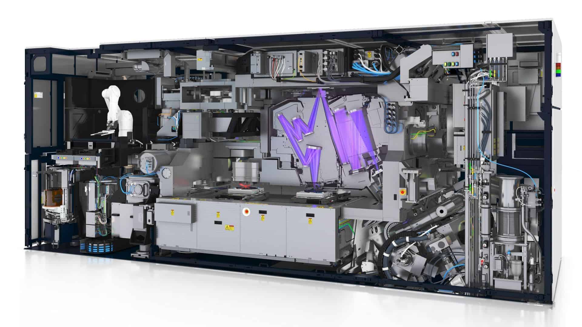
EUV machines are the most advanced tools used in semiconductor manufacturing. They use extreme ultraviolet light to etch tiny patterns onto silicon wafers, enabling the production of smaller and more powerful chips. Each EUV machine can cost from about $150 million to $380 million, and ASML is the only company that makes them.
These systems are essential for producing chips at cutting-edge nodes, such as those used by Intel, TSMC, and Samsung. High-NA EUV models push this even further, allowing finer features and higher transistor density while reducing the need for complex multi-patterning steps. However, their size, cost, and technical demands make them challenging to adopt.
The technology shapes how chip designs evolve and how fabs plan their production lines. From the optics that reflect EUV light to the vacuum chambers that keep it stable, every part of the machine must meet extreme precision standards. This combination of performance and complexity explains why EUV is both a breakthrough and a major investment for the semiconductor industry.
What They Are, Costs, and Lithography Technology
1. What is an EUV Machine?
An EUV machine (Extreme Ultraviolet Lithography system) is a highly advanced semiconductor manufacturing tool used to print the smallest possible features on microchips. It uses 13.5 nm wavelength extreme ultraviolet light to etch circuits onto silicon wafers, enabling the production of chips at 3nm, 2nm, and beyond.
- Manufacturer: ASML (Netherlands) is currently the only company in the world producing commercial EUV lithography machines.
- Purpose: Enables higher transistor density, faster chips, and lower power consumption.
- Users: TSMC, Samsung, Intel, and other leading fabs.
2. How EUV Lithography Works
EUV lithography replaces older DUV (Deep Ultraviolet) systems by using shorter wavelengths for higher precision.
Basic process:
- EUV Light Generation – A high-powered laser hits a tin droplet, creating plasma that emits EUV light.
- Reflection Optics – Since EUV light is absorbed by most materials, mirrors (not lenses) are used.
- Mask Projection – The light is projected through a mask containing the chip design.
- Wafer Exposure – The pattern is transferred to a light-sensitive photoresist on the silicon wafer.
- Etching & Processing – The wafer undergoes chemical processes to complete the circuit patterns.
3. EUV Machine Costs
EUV systems are some of the most expensive machines ever built.
| Model / Generation | Wavelength | Node Capability | Approx. Cost (USD) | Status |
|---|---|---|---|---|
| ASML NXE:3400B | 13.5 nm | 7nm / 5nm | $150M–$180M | In use since 2018 |
| ASML NXE:3600D | 13.5 nm | 5nm / 3nm | $200M–$250M | Widely used by TSMC & Samsung |
| ASML NXE:3800E | 13.5 nm | 3nm / 2nm | $250M–$300M | Latest high-volume model (2024) |
| ASML High-NA EUV (EXE:5000) | 13.5 nm (High-NA) | 2nm / 1.4nm | $350M–$380M | Early deployment in 2025 |
Key facts:
- Each machine weighs ~180 tons and requires a Boeing 747 or multiple trucks to transport.
- Installation takes months and requires a controlled cleanroom environment.
- ASML has sold ~140 EUV machines in the past decade (source).
4. Latest Developments (2024–2025)
- High-NA EUV Rollout: ASML’s EXE:5000 High-NA EUV systems are entering production in 2025, enabling 2nm and 1.4nm nodes with fewer process steps.
- China’s Push for Domestic EUV: The Chinese Academy of Sciences has launched a dedicated EUV R&D team to reduce reliance on ASML amid export restrictions (source).
- Cost Reduction Efforts: Industry research is focusing on lowering EUV operational costs and improving uptime (source).
- Increased Adoption: More fabs, including smaller semiconductor manufacturers, are exploring EUV integration thanks to new business models (Semiconductor Engineering).
5. Challenges with EUV Technology
- High Cost – Both purchase price and maintenance are expensive.
- Complexity – Requires ultra-clean environments and precision alignment.
- Throughput Limitations – EUV exposure speed is slower than some DUV processes.
- Supply Chain Bottlenecks – ASML’s production capacity is limited, causing long lead times.
6. The Future of EUV
- High-NA EUV will be the standard for sub-2nm chips by 2026.
- Hybrid Lithography (EUV + DUV) will remain common to balance cost and performance.
- Potential EUV Alternatives like E-beam lithography and nanoimprint lithography are being researched, but none are near mass production readiness.
💡 Bottom line:
EUV lithography is the backbone of modern semiconductor manufacturing. While expensive and complex, it is essential for producing the world’s most advanced chips — from smartphones to AI supercomputers. With High-NA EUV now rolling out, the next leap in chip performance is already underway.
Key Takeaways
- EUV machines use extreme ultraviolet light to create advanced semiconductor chips.
- ASML is the only company producing these machines, with prices up to $380 million.
- High-NA EUV enables smaller features but adds cost and design challenges.
Frequently Asked Questions
EUV lithography machines use short-wavelength light to create extremely fine patterns on silicon wafers. They enable smaller transistors, higher chip density, and improved performance while introducing new cost, engineering, and operational demands.
How do extreme ultraviolet (EUV) lithography machines contribute to semiconductor manufacturing?
EUV machines project patterns onto wafers at a wavelength of 13.5 nanometers. This allows chipmakers to produce features smaller than those possible with deep ultraviolet (DUV) systems.
They are used in high-volume production of advanced logic and memory chips, supporting the continued scaling of transistor sizes.
What are the main technological advancements in EUV lithography over the past decade?
Light sources have become more powerful, improving throughput. Optical systems have gained higher precision, and resist materials have been optimized for better pattern fidelity.
The introduction of High Numerical Aperture (High-NA) EUV has increased resolution from about 13 nm to around 8 nm.
Can you compare the costs and benefits of EUV lithography with traditional photolithography?
EUV machines cost between $150 million and $380 million, far higher than DUV systems. Operating costs are also higher due to complexity and maintenance needs.
In return, EUV enables finer features, reducing the number of patterning steps compared to DUV, which can lower process complexity for advanced nodes.
What are the challenges associated with implementing EUV lithography in chip fabrication?
Throughput is lower than with DUV, making production speed a concern. The machines require a near-perfect vacuum and precise alignment.
High costs limit adoption to large semiconductor companies, and maintenance demands can disrupt production schedules.
How does EUV lithography impact the scalability of chip production?
EUV allows continued transistor scaling beyond the limits of DUV, supporting Moore’s Law. It reduces the need for multiple patterning steps, which can simplify manufacturing at smaller nodes.
However, limited availability of machines and high capital costs can slow large-scale deployment.
What is the expected lifespan of current EUV lithography machines and their maintenance requirements?
An EUV machine can operate for many years if maintained properly, often exceeding a decade in service.
Maintenance involves regular calibration, replacement of critical parts, and downtime for system checks. These tasks require specialized engineers and can be costly.

