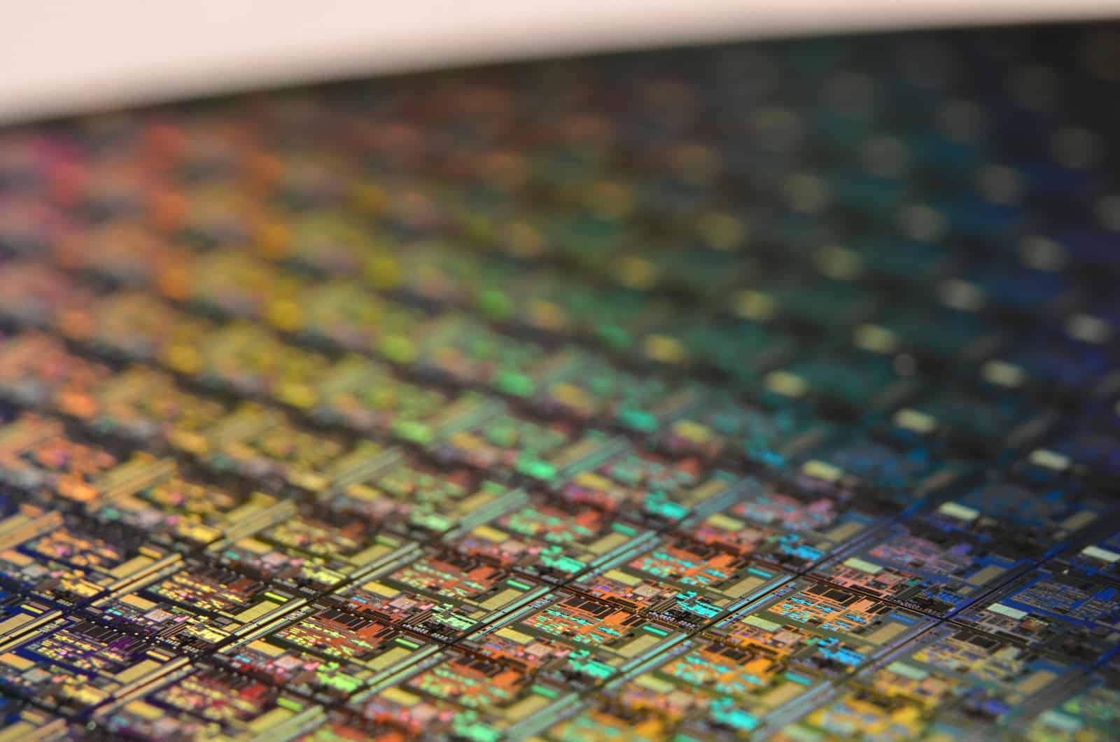
The shift from FinFET to gate-all-around (GAA) transistors marks one of the biggest changes in chip design in years. Instead of wrapping the gate on three sides like FinFETs, GAA transistors surround the channel completely, giving chipmakers tighter control over current and leakage. This design boosts chip performance, increases transistor density, and lowers power use, making it a direct path forward as Moore’s Law slows.
These improvements matter across many areas of technology. Smaller and more efficient transistors support faster CPUs and GPUs, extend battery life in mobile devices, and power the growth of AI accelerators. As system-on-chip (SoC) designs shift toward chiplets, the benefits of GAA remain critical because the most advanced components still demand the highest density and performance.
The move to GAA also gives the semiconductor industry a clearer future roadmap. With scaling challenges mounting, this architecture provides a way to keep progress steady without relying only on shrinking process nodes. Companies adopting GAA at 3nm and beyond show how it can extend innovation while balancing efficiency and cost.
Gate-All-Around (GAA)
The Gate-All-Around (GAA) transistor represents the next major evolution in semiconductor device architecture after the FinFET. As the industry moves into nodes below 5 nm, traditional FinFETs face challenges in controlling leakage and short-channel effects. GAA transistors address these limitations by completely surrounding the channel with the gate, offering superior electrostatic control and scalability.
GAA designs are now central to advanced process nodes such as Samsung’s 3GAE (3 nm) and TSMC’s N2 (2 nm) technologies.
What Is a Gate-All-Around (GAA) Transistor?
A GAA transistor is a type of Field-Effect Transistor (FET) in which the gate material wraps entirely around the channel region.
This full enclosure provides uniform control over the channel, minimizing leakage current and improving switching efficiency.
🧩 Structure Comparison
| Feature | FinFET | GAA (Nanosheet/Nanowire FET) |
|---|---|---|
| Gate coverage | 3 sides of the channel | All 4 sides of the channel |
| Channel shape | Fin-like vertical structure | Horizontal nanosheets or nanowires |
| Electrostatic control | Good | Excellent |
| Scaling potential | Limited below 5 nm | Extends scaling to ~1 nm and beyond |
Key Innovations in GAA Technology
🔹 1. Nanosheet and Nanowire Channels
GAA transistors use stacked nanosheets or nanowires as channels.
- Nanosheets offer higher drive current due to wider channels.
- Nanowires provide better electrostatic control but lower current density.
Modern designs often use nanosheet FETs (NSFETs) for optimal performance balance.
🔹 2. Dynamic Channel Width Modulation
The width of the nanosheet channels can be tuned during fabrication, allowing power-performance optimization within a single chip.
This flexibility enables multi-Vt (threshold voltage) designs for both high-performance and low-power applications.
🔹 3. Improved Electrostatic Control
The gate-all-around geometry virtually eliminates short-channel effects, allowing lower operating voltages and reduced leakage currents — a key enabler for sub-3 nm nodes (ResearchGate, 2024).
🔹 4. Material and Process Innovations
GAA fabrication leverages:
- Epitaxial growth of Si/SiGe for nanosheet formation
- Atomic Layer Deposition (ALD) for precise gate oxide control
- Selective etching to release stacked channels
These process innovations ensure precise nanoscale geometry and uniformity (AnySilicon, 2024).
Advantages Over FinFETs
| Advantage | Description |
|---|---|
| Better electrostatic control | Reduces short-channel effects and improves subthreshold slope |
| Lower leakage current | Enhances energy efficiency |
| Scalability | Enables continued Moore’s Law scaling below 3 nm |
| Higher drive current | Improves performance for high-speed logic |
| Design flexibility | Adjustable channel width for power-performance trade-offs |
Challenges and Limitations
Despite their promise, GAA transistors present manufacturing and integration challenges:
- Complex fabrication: Multi-layer nanosheet stacks require precise etching and alignment.
- Thermal management: Increased power density can lead to heat dissipation issues.
- Yield and variability: Tight process tolerances affect large-scale production.
- Integration with existing design flows: Transitioning from FinFET to GAA requires new design rules and EDA tool support.
(Luciano D’Agnillo, Challenges and Opportunities with GAA Transistors)
Industry Adoption and Outlook
- Samsung began mass production of GAA-based 3 nm chips in 2022 (3GAE), with improved power efficiency and performance.
- TSMC plans to introduce N2 GAA technology by 2025, focusing on nanosheet-based GAAFETs.
- Intel’s RibbonFET (part of Intel 20A) is its GAA implementation, expected to debut in the mid-2020s (Nature, 2023).
Future Impact
GAA transistors are expected to:
- Extend Moore’s Law beyond traditional FinFET limits
- Enable AI and high-performance computing (HPC) chips with better energy efficiency
- Support heterogeneous integration and 3D chip stacking
- Drive the development of sub-1 nm process nodes (IPRally, 2024)
Gate-All-Around (GAA) transistors mark a pivotal step in semiconductor evolution.
By fully surrounding the channel, they deliver superior electrostatic control, energy efficiency, and scalability — essential for the next generation of computing.
While fabrication complexity remains a challenge, ongoing innovations in materials, processes, and design automation are paving the way for widespread adoption.
📚 Key References
- A Review of the Gate-All-Around Nanosheet FET Process Opportunities – ResearchGate
- Challenges and Opportunities with Gate-All-Around Transistors – Luciano D’Agnillo
- Exploring Gate-All-Around (GAA) Transistors – DiverseDaily
- The Ultimate Guide to GAA – AnySilicon
- The Next Generation of Gate-All-Around Transistors – Nature
- From FinFET to GAAFET – IPRally
Key Takeaways
- Gate-all-around transistors improve chip performance and efficiency.
- The design supports both traditional SoCs and chiplet-based systems.
- GAA helps extend scaling beyond the limits of FinFET designs.
Frequently Asked Questions
Gate-All-Around (GAA) transistors mark a shift in how chips are designed and built. They offer better control of current, enable smaller nodes, and present new challenges in manufacturing and adoption by foundries.
What are the advantages of Gate-All-Around (GAA) technology over FinFET?
GAA transistors surround the channel on all sides, unlike FinFETs that cover only three. This gives stronger electrostatic control, reduces leakage, and allows lower operating voltage.
They also scale better to smaller nodes, making them more efficient in terms of power and performance.
How does the Gate-All-Around process flow differ from traditional semiconductor fabrication processes?
The process replaces fin structures with nanosheets or nanowires wrapped by the gate. This requires new steps for shaping and stacking the channels.
It still uses extreme ultraviolet (EUV) lithography, but the channel geometry and integration flow differ from FinFET fabrication.
What are the unique manufacturing challenges associated with GAA transistors?
Controlling nanosheet dimensions with precision is difficult. Variations in thickness or alignment can affect performance and yield.
Integration of multiple stacked layers also adds complexity to the process. Manufacturers must maintain uniformity while keeping costs under control.
In what ways is GAA technology being implemented by leading semiconductor companies like TSMC, Samsung, and Intel?
Samsung has already introduced GAA at the 3nm node in commercial production. TSMC plans to use GAA, called “nanosheet” technology, at its 2nm node.
Intel is developing RibbonFET, its own GAA design, which is expected to appear in its next-generation process technologies.
How does GAA FET design improve electrical performance and scalability?
The full gate wrap improves electrostatic control, which reduces short-channel effects. This allows transistors to switch faster and consume less power.
Better scaling means higher transistor density, enabling more functions on a single chip without raising power use.
What are the latest developments in GAA transistor fabrication techniques?
Foundries are refining nanosheet stacking methods to improve uniformity and yield. Research also explores new channel materials, such as III-V semiconductors, for higher mobility.
EUV lithography continues to play a central role, with ongoing advances in patterning accuracy for sub-3nm nodes.

